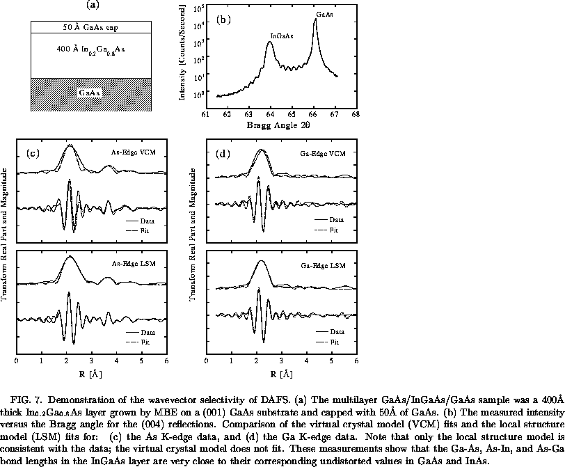
A 400Å thick strained ![]() layer,
grown epitaxially on GaAs, was chosen for this study. XAFS
experiments could not be used to study the InGaAs local structure in
this sample because of strong interfering signals from the GaAs
substrate and cap. The structure of the GaAs/InGaAs/GaAs sample is
shown in Fig. 7a.
layer,
grown epitaxially on GaAs, was chosen for this study. XAFS
experiments could not be used to study the InGaAs local structure in
this sample because of strong interfering signals from the GaAs
substrate and cap. The structure of the GaAs/InGaAs/GaAs sample is
shown in Fig. 7a.
The lattice spacing of the 400Å InGaAs layer was larger than the
lattice spacing of the GaAs substrate and cap, and the InGaAs
diffraction peak was well separated from the GaAs peak.
Figure 7b shows the measured x-ray diffraction pattern as a
function of the Bragg angle ![]() near the GaAs (004) Bragg peak
for a photon energy of
near the GaAs (004) Bragg peak
for a photon energy of ![]() eV. The intense peak at
eV. The intense peak at
![]() was produced by the GaAs substrate, while
the broad peak at
was produced by the GaAs substrate, while
the broad peak at ![]() was produced by the
InGaAs layer. The InGaAs peak is broad and has ``subsidiary'' side
lobes, due to the finite thickness of the InGaAs layer. Because the
InGaAs and GaAs peaks were well separated in
was produced by the
InGaAs layer. The InGaAs peak is broad and has ``subsidiary'' side
lobes, due to the finite thickness of the InGaAs layer. Because the
InGaAs and GaAs peaks were well separated in ![]() , the
Ga and As DAFS signals from the InGaAs peak could be
measured without interference from the Ga and As in the substrate.
, the
Ga and As DAFS signals from the InGaAs peak could be
measured without interference from the Ga and As in the substrate.